Fitxategi:Wafer flats convention v2.svg

Bereizmen handikoa (SVG fitxategia, nominaldi 150 × 150 pixel, fitxategiaren tamaina: 13 KB)
Fitxategi hau Wikimedia Commonsekoa da. Hango deskribapen orriko informazioa behean duzu. |
Laburpena
| Deskribapena |
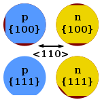
Wafer flats convention, based on Image:Wafer flats convention.PNG Conventional meaning of flats in semiconductor wafers. Red denotes material that has been removed. Wafer orientation is the orientation of the crystallographic plane in which the crystal grew. Wafer type indicated the type of doping.
|
| Data | |
| Jatorria |
self-made, Fitxategi hau (bektore-irudia) hau Inkscape-ekin sortu da .
. |
| Egilea | Twisp |
| Beste bertsioak | Wafer flats convention.PNG |
Lizentzia
| Nik, lan honen egile eskubideen jabeak, lan hau domeinu publikoan jartzen dut. Mundu osoan du eragina honek. Estatu batzuetan beharbada hori ez da legez posible izango. Halakoetan: Edonori ematen diot lan hau edozertarako erabiltzeko eskubidea, inolako baldintzarik gabe, legeak nahitaez ezarritako baldintzak izan ezik. |
Fitxategiaren historia
Data/orduan klik egin fitxategiak orduan zuen itxura ikusteko.
| Data/Ordua | Iruditxoa | Neurriak | Erabiltzailea | Iruzkina | |
|---|---|---|---|---|---|
| oraingoa | 23:40, 24 iraila 2013 | | 150 × 150 (13 KB) | Cepheiden | fixed position of secondary flat Silicon processing for the VLSI era - Vol. 1 - Process technology; S Wolf; RN Tauber - Lattice Press; 1986; ISBN 096167237; p. 23 |
| 02:37, 23 abendua 2008 |  | 150 × 150 (13 KB) | Inductiveload | Added arrow indication <110> direction and enlarged flats so they can be easily seen | |
| 23:17, 29 otsaila 2008 |  | 150 × 150 (9 KB) | Twisp | ||
| 23:13, 29 otsaila 2008 |  | 150 × 150 (9 KB) | Twisp | ||
| 23:06, 29 otsaila 2008 |  | 150 × 150 (8 KB) | Twisp | ||
| 22:59, 29 otsaila 2008 |  | 150 × 150 (8 KB) | Twisp | ||
| 20:09, 29 otsaila 2008 |  | 150 × 150 (9 KB) | Twisp | {{Information |Description= Wafer flats convention, based on Image:Wafer flats convention.PNG Conventional meaning of ''flats'' in semiconductor wafers. Black denotes material that has been removed. Wafer orientation is |
Irudira dakarten loturak
Hurrengo orrialdeek dute fitxategi honetarako lotura:
Fitxategiaren erabilera orokorra
Hurrengo beste wikiek fitxategi hau darabilte:
- ca.wikipedia.org proiektuan duen erabilera
- cs.wikipedia.org proiektuan duen erabilera
- de.wikipedia.org proiektuan duen erabilera
- en.wikipedia.org proiektuan duen erabilera
- es.wikipedia.org proiektuan duen erabilera
- et.wikipedia.org proiektuan duen erabilera
- fi.wikipedia.org proiektuan duen erabilera
- it.wikipedia.org proiektuan duen erabilera
- it.wikibooks.org proiektuan duen erabilera
- ja.wikipedia.org proiektuan duen erabilera
- ko.wikipedia.org proiektuan duen erabilera
- nl.wikipedia.org proiektuan duen erabilera
- pl.wikipedia.org proiektuan duen erabilera
- ro.wikipedia.org proiektuan duen erabilera
- sk.wikipedia.org proiektuan duen erabilera
- uk.wikipedia.org proiektuan duen erabilera
- www.wikidata.org proiektuan duen erabilera