Fitxategi:PCB design and realisation smt and through hole.png
Aurreikuspen honen neurria: 800 × 427 pixel. Bestelako bereizmenak: 320 × 171 pixel | 640 × 341 pixel | 1.024 × 546 pixel | 1.280 × 683 pixel | 3.000 × 1.600 pixel.
Bereizmen handikoa ((3.000 × 1.600 pixel, fitxategiaren tamaina: 2,74 MB, MIME mota: image/png))
Fitxategi hau Wikimedia Commonsekoa da. Hango deskribapen orriko informazioa behean duzu. |
| Deskribapena |
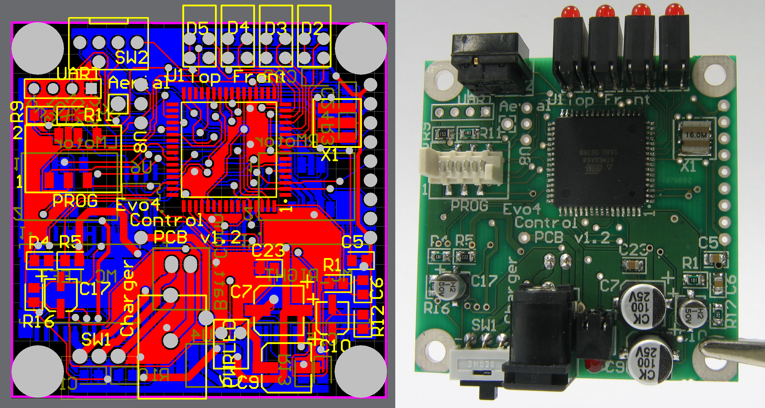
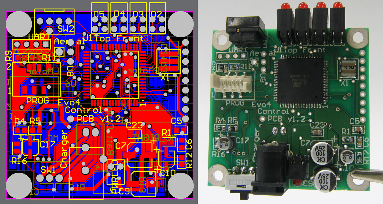
English: This picture shows (left) a printed circuit board (PCB) layout, created on a computer and (right) the manufactured board, populated with parts. Both through-hole and surface mounts components have been used; the board is double-sided, with through-hole plating, green solder resist, white solder paste (visible on unsoldered holes, such as the four corner mounting holes and the nine holes down the right hand side of the board) and white silkscreen printing.
Italiano: Progetto di un circuito stampato a sinistra e realizzazione a destra.
Deutsch: Links das im CAD erstellte Layout einer Leiterplatte, in dem die verschiedenen Lagen mit unterschiedlichen Farben dargestellt sind. Rechts die daraus hergestellte und mit Bauelementen bestückte Leiterplatte.
Español: A la izquierda la imagen de la PCB diseñada por ordenador y a la derecha la PCB manufacturada y montada.
Svenska: Datordesign av ett mönsterkort (vänster) och det färdiga kretskortet (höger)
中文:印刷電路板
Magyar: A baloldalon egy NYÁK CAD program segítségével tervezett rajza, a jobboldalon pedig a rajznak megelelően elkészített panel látható.
Bahasa Indonesia: Foto dari desain sirkuit dan realisasinya
한국어: 컴퓨터로 설계된 인쇄회로기판 (왼쪽) 및 기판과 부품이식된 실장 (오른쪽). 기판은 홀로 통하는 도금, 녹색 땝납 저항, 흰 땝납 페이스트, 흰 실크스크린 프린트가 있는, 양면이다. 양쪽 표면 실장과 홀로 통하는 부품은 사용되었다. |
||
| Data | |||
| Jatorria | Photographed by User:Mike1024 | ||
| Egilea | User Mike1024 | ||
| Lizentzia (Fitxategi hau berrerabiltzen) |
|
Fitxategiaren historia
Data/orduan klik egin fitxategiak orduan zuen itxura ikusteko.
| Data/Ordua | Iruditxoa | Neurriak | Erabiltzailea | Iruzkina | |
|---|---|---|---|---|---|
| oraingoa | 21:10, 2 otsaila 2007 | | 3.000 × 1.600 (2,74 MB) | Mike1024 | {{Information| |Description=This picture shows (left) a printed circuit board (PCB) layout, created on a computer and (right) the manufactured board, populated with parts. Both through-hole and surface mounts components have been used; the board is double |
Irudira dakarten loturak
Hurrengo orrialdeek dute fitxategi honetarako lotura:
Fitxategiaren erabilera orokorra
Hurrengo beste wikiek fitxategi hau darabilte:
- ast.wikipedia.org proiektuan duen erabilera
- ca.wikipedia.org proiektuan duen erabilera
- de.wikipedia.org proiektuan duen erabilera
- en.wikipedia.org proiektuan duen erabilera
- es.wikipedia.org proiektuan duen erabilera
- et.wikipedia.org proiektuan duen erabilera
- fr.wikipedia.org proiektuan duen erabilera
- fr.wiktionary.org proiektuan duen erabilera
- hi.wikipedia.org proiektuan duen erabilera
- hi.wikiversity.org proiektuan duen erabilera
- hu.wikipedia.org proiektuan duen erabilera
- id.wikipedia.org proiektuan duen erabilera
- it.wikipedia.org proiektuan duen erabilera
- ja.wikipedia.org proiektuan duen erabilera
- ko.wikipedia.org proiektuan duen erabilera
- ne.wikipedia.org proiektuan duen erabilera
- pt.wikipedia.org proiektuan duen erabilera
- ru.wikipedia.org proiektuan duen erabilera
- sv.wikipedia.org proiektuan duen erabilera
- vi.wikipedia.org proiektuan duen erabilera
- zh.wikipedia.org proiektuan duen erabilera